Wafer Inspection | Environmental XPRT
Articles & Whitepapers
-
Teron SL670e and Teron SL670e XP: EUV Reticle Quality Control
Extreme ultraviolet (EUV) lithography is a key technology inflection for the semiconductor industry. While shifting the scanner wavelength to EUV has enabled printing of the smaller pattern features required for ≤5nm design node chips, it has also added tremendous complexity to the equipment, reticles, resists and other infrastructure required to support EUV lithography. New defect mechanisms ...
-
What is an Aspheric Lens?
Aspheric lenses (or more simply, aspheres) are used in a wide variety of applications as a way to optimize optical performance while ensuring an efficient design. They are characterized by a radius ...
News
-
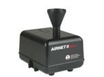
Aerosol Particle Monitoring Inside of Semiconductor Process Tools
Introduction Contamination poses a significant threat to semiconductor manufacturing processes, impacting yield and revenue. This blog explores the pivotal role of real-time aerosol particle monitoring in semiconductor manufacturing, specifically ...
Equipment & Solutions
-
Showcase
Semiconductor Wafer Stress Measurement
Faced with the increasing complexity of semiconductor manufacturing processes, IDMs and foundries rely on high performance production-worthy transparent film metrology for fabwide process control. Metrosemi’s MetroStress 101 of metrology systems deliver superior measurement accuracy, repeatability and tool-to-tool matching on a highly reliable and flexible platform. Utilizing ...


